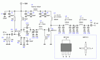
Schematic Diagram:
Parts List:
R1, R2, R3, R4 = 100
R5 = 10k
C1 = 220uF
C2, C3, C4, C5, C6, C7 = 100nF
C8, C9 = 1nF
C10, C11, C12 = 22pF
C13, C14, C15, C16 = 15pF
C17, C18 = 10pF C
19, C20 =(Variable capacitor 5-25pF)
L1, L2 = 10uH
L3 = 45nH 2 turns diam 5mm (wire = 0.8mm)
L4 = 27uH (Can be 10uH-100uH)
L5 = > 500nH 10-15 turns diam 6.5mm (wire = 0.8mm)
L6, L7 = 100nH 3 turns diam 6.5mm (wire = 0.8mm)
Q1 = BFG193
Q2 = MRF313, 2N3866, 2N4427
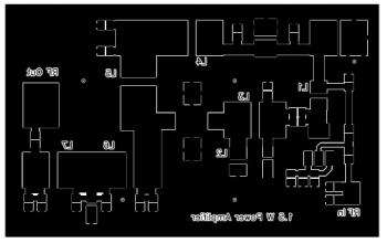
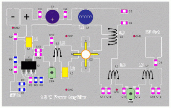
PCB Design:
Complete explanation about this RF amplifier circuit, go to this page
About RF Amplifier
An RF power amplifier is a type of electronic amplifier which is utilised to convert a low-power radio-frequency signal into a larger signal of significant power, usually for driving the antenna of a transmitter. It is usually optimized to have high efficiency, high output Power (P1dB) compression, good gain, good return loss on the input and output, and optimum heat dissipation.
The basic applications of the RF power amplifier include driving to another high power source, driving a transmitting antenna, microwave heating, and exciting resonant cavity structures. Among these applications, driving transmitter antennas is most well known.
More explanation about power audio amplifier can be found at wikipedia.org
This is a demonstration about 01A RF Amplifier which is build used old tube component to amplify the signal. An RF power amplifier is a type of electronic amplifier which is utilised to convert a low-power radio-frequency signal into a larger signal of significant power, usually for driving the antenna of a transmitter. It is usually optimized to have high efficiency, high output Power (P1dB) compression, good gain, good return loss on the input and output, and optimum heat dissipation.
The basic applications of the RF power amplifier include driving to another high power source, driving a transmitting antenna, microwave heating, and exciting resonant cavity structures. Among these applications, driving transmitter antennas is most well known.
More explanation about power audio amplifier can be found at wikipedia.org
Watch the video:


No comments:
Post a Comment