Several of these amplifiers have been built and exhibit similar performance. Al has been using his amplifier on each of the HF bands, logging well over 500 contacts in 18 months. Signal reports indicate a noticeable improvement in readability (about two S units on average) over his 5 W rig. No indications of instability, CW key clicks or distortion on SSB have been reported. To make it easy for you to duplicate this project, PC boards and parts kits are available, all at a cost of about $100!
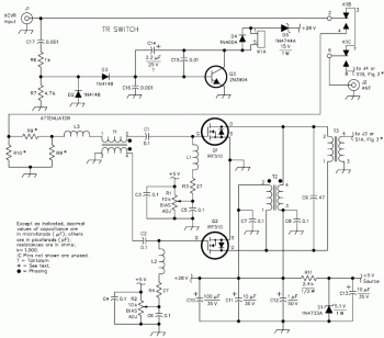
Schematic diagram of the MOSFET all-band HF amplifier. Unless otherwise specified, resistors are 1/4 W, 5% tolerance carbon-composition or film units. Equivalent parts can be substituted.
Components List:
C1-C8 = 0.1 μF chip (140-CC502Z104M)
C9 = 47 pF chip (140-CC502N470J)
C10 = 100 μF, 35 V (140-HTRL35V100)
C11, C13 = 15 μF, 35 V (140MLR35V10)
C12 = 1 μF, 50 V (140-MLRL50V1.0)
C14 = 2.2 μF, 35 V tantalum (581-2.2M35V)
C15 = 0.01 μF chip (140-CC502B103K)
C16, C17 = 0.001 μF chip (140-CC502B102K)
D1 = 1N4733A, 5.1 V, 1 W Zener diode (583-1N4733A)
D4 = 1N4004A(583-1N4004A)
D2, D3 = 1N4148 (583-1N4148)
D5 = 1N4744A, 15 V, 1 W Zener diode (583-1N4744A)
J1, J2 = SO-239 UHF connector (523-81-120)
K1 = 12 V DPDT, 960 Ω coil, 12.5 mA (431-OVR-SH-212L)
L1, L2 = 91/2 turns #24 enameled wire, closely wound 0.25-in. ID
L3 = 31/2 turns #24 enameled wire, closely wound 0.190-in. ID
Q1, Q2 = IRF510 power MOSFET (570-IRF510)
Q3 = 2N3904 (610-2N3904)
R1, R2 = 10 kΩ trim pot (323-5000-10K)
R3, R4 = 27 Ω, 1/2 W (293-27)
R6 = 1 kΩ chip (263-1K)
R7 = 4.7 kΩ chip (263-4.7K)
R8 = 130 Ω, 1 W (281-130); for 7 dB pad (5 W in, 1 W out)
R9 = 43 Ω, 2 W (282-43); for 7 dB pad (5 W in, 1 W out)
R10 = 130 Ω, 3 W (283-130); for 7 dB pad (5 W in, 1 W out)
R8, R10—300 Ω, 1/2 W (273-300); for 3 dB pad (2 W in, 1 W out)
R9 = 18 Ω, 1 W (281-18); for 3 dB pad (2 W in, 1 W out)
R11 = 2.4 kΩ, 1/2 W (293-2.4K)
T1 = 10 bifilar turns #24 enameled wire on an FT-50-43 core.
T2 = 10 bifilar turns #22 enameled wire on two stacked FT-50-43 cores.
T3 = Pri 2 turns, sec 3 turns #20 Teflon covered wire on BN-43-3312 balun core.
Low-cost broadband HF amplifier based MOSFET IRF510, download the complete explanation here
About RF Amplifier
An RF power amplifier is a type of electronic amplifier which is utilised to convert a low-power radio-frequency signal into a larger signal of significant power, usually for driving the antenna of a transmitter. It is usually optimized to have high efficiency, high output Power (P1dB) compression, good gain, good return loss on the input and output, and optimum heat dissipation.
The basic applications of the RF power amplifier include driving to another high power source, driving a transmitting antenna, microwave heating, and exciting resonant cavity structures. Among these applications, driving transmitter antennas is most well known.
More explanation about power audio amplifier can be found at wikipedia.org
This is a demonstration about 01A RF Amplifier which is build used old tube component to amplify the signal. An RF power amplifier is a type of electronic amplifier which is utilised to convert a low-power radio-frequency signal into a larger signal of significant power, usually for driving the antenna of a transmitter. It is usually optimized to have high efficiency, high output Power (P1dB) compression, good gain, good return loss on the input and output, and optimum heat dissipation.
The basic applications of the RF power amplifier include driving to another high power source, driving a transmitting antenna, microwave heating, and exciting resonant cavity structures. Among these applications, driving transmitter antennas is most well known.
More explanation about power audio amplifier can be found at wikipedia.org
Watch the video:

No comments:
Post a Comment